How to Manufacture Semiconductor Chips?
The increasing adoption of digitization coupled with enhanced connectivity is rapidly accelerating the demand for modern electronics. The global consumer electronics market size was valued at over USD1 trillion and is anticipated to grow at a CAGR of 8% from 2021 to 2027 with increasing internet penetration. All modern electronics require semiconductors that sit in the heart of integrated circuits and specialized components, from the smartphone in your pocket to cutting-edge vehicles. Made using raw materials such as silicon, germanium, and other pure materials, semiconductor lies between a conductor and an insulator to manage and control current flow in electronics.
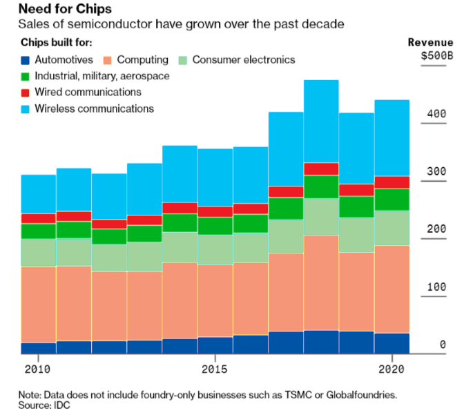
Rapidly increasing appetite for consumer electronics, expansion of 5G, and advancements in technology are exploding the demand for processors. According to International Data Corporation (IDC), the global semiconductor market is expected to reach a value of USD600 billion by 2025. Currently, there is a huge global shortage of semiconductors due to supply chain shortages and a sudden spike in the usage of electronics since the pandemic. The semiconductor industry is substantially ramping up its fab capacity utilization to meet the growing demand for chips.

Semiconductor manufacturing is a costly, complex, and highly disciplinary procedure which involves physics, chemistry, electricity, metallurgy, and more. Manufacturing chips is one of the most R&D- and capital-intensive manufacturing processes on earth. Around 1400 process steps are involved in the overall manufacturing of just the semiconductor wafers alone, and each phase includes the use of a variety of highly sophisticated tools and machines. On average, manufacturing a semiconductor wafer takes up to 12 weeks, whereas a finished chip can require 26 weeks.

From Silicon to Semiconductor: An Overview
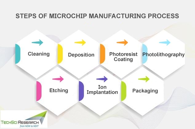
A semiconductor chip is an electric circuit built up in a series of nanofabrication processes performed on the surface of substrates (wafers) composed of highly pure single crystal silicon. The production of a microchip involves adding impurities to the base element in a process called “doping” to adjust the conductance or inductance of the outcome, based on the type and intensity of impurities added. Here are the seven crucial steps involved in the manufacturing of semiconductors.
· Cleaning
Silicon wafers forming the base of the microchip are cleaned by a solvent and followed by a deionized water (DI) rinse and blow-dry. This is the first and most crucial step of semiconductor manufacturing, as even slight contamination can cause defects in the circuit. Generally, chemical agents remove the contamination, varying from ultra-fine particles to minute amounts of metallic residues generated during the production process or natural oxide layer formed due to air exposure. The final wafer cleaning step involves a Hydrofluoric Acid dip for two minutes to remove the silicon oxide layer. Then, the wafer is put under running DI water, and a wettability test is conducted to confirm whether the cleaning was successful or needed more. If the water turns into little beads and rolls off, then the wafers are considered good to go for further processing.
- Deposition
The semiconductor chip manufacturing process initiates with a silicon wafer. Wafers are sliced from a salami-shaped bar made of 99.99% pure silicon and polished until they become highly smooth. Depending on the type of structure being created, thin films of dielectric (insulating) and metal (conducting) materials are deposited on the wafer surface to build a microchip. This process is known as deposition. There are multiple ways to perform deposition: sputtering, electrodeposition, chemical vapor deposition, and thermal deposition. The kind of technique used for deposition depends upon the process node, type of chip, and the amount of time needed to do the deposition.
Sputtering involves the bombarding of ions on the target materials, which knocks off atoms and molecules that are further deposited on the wafer surface. Electrodeposition is used to form copper wire layers. In contrast, chemical vapor deposition includes special gases that cause a chemical reaction to generate molecules that are then deposited on the wafer surface to form a film. Thermal oxidation includes heating up of wafer to form a silicon oxide film on the wafer surface.
- Photoresist coating
The semiconductor wafer is covered with a light-sensitive coating called ‘photoresist’ or ‘resist’ that blocks everything not meant to be exposed to ultraviolet light. The resist coating can be positive or negative, depending upon the chemical structure of the material and the way that the resist reacts with light. With positive resist, the area exposed to light changes its structure, whereas with negative resist, the areas hit by light polymerize and become more difficult to dissolve. Generally, a positive resist is used in semiconductor manufacturing due to its higher resolution capabilities. It is crucial to have a resist coating method to have a uniform coating of photoresist over the surface of the substrate. Several options available for resist coating include spin coating, spray coating, dip coating, inkjet printing, and slot-die coating.
- Photolithography
Lithography is a crucial step in the chipmaking process which involves transferring patterns of geometric shapes in a mask to a thin layer of radiation-sensitive material called resist. This process determines just how small the transistors on the chips can be. The geometric shapes and patterns on a semiconductor make up the complex structures that allow dopants to complete a circuit to fulfill a technological purpose. During this process, the semiconductor wafer is inserted into a lithography machine, where it is exposed to deep UV lights to produce the finest details of a chip. The light projected through the ‘reticle’ causes a chemical change that enables the pattern to be replicated on the resist. A complementary metal-oxide-semiconductor (CMOS) wafer can undergo the photolithographic cycles as many as 50 times.
- Etching
The etching process is used to eliminate the degraded resist to reveal the intended pattern. During this procedure, the wafer is baked and developed. A developer is sprayed on the water, which dissolves the areas exposed to the light and reveals a 3D pattern of open channels. Etching process can be done in two ways, wet etching and dry etching. During wet etching, the exposed thin film on the surface layer is dissolved using chemicals such as hydrofluoric or phosphoric acid, which is then later removed. In dry etching, the wafer is exposed to dry gases with ionized atoms to remove the film layer. Etching must be done in a way that it precisely and consistently forms increasingly conductive features and does not hinder the integrity and stability of the chip. Advanced etch technology enables semiconductor manufacturers to use double, quadruple, and spacer-based patterning to create tiny features.
- Ion Implantation
This step involves the implantation of impurities to provide the silicon substrate semiconducting properties. Generally, impurities such as phosphor, arsenic, or boron are implanted in the wafers that are shot into the wafer in a bullet-like fashion. Sacrificial films prevent the ions from being shot at the unwanted places of the wafer. Directing electrically charged ions (positive or negative) into the silicon crystal controls the flow of electricity and allows the creation of transistors. After this procedure, the remaining sections of resist are not etched or ionized.
- Packaging
Packaging is a crucial part of semiconductor manufacturing and design as it can affect the power, performance, and cost on a macro level and functionality on a micro level. The semiconductor wafer is sliced and diced with a diamond saw to get the individual chips out of the wafer. Semiconductor chips are cut from the wafer and are referred to as ‘dies,’ which can vary in different sizes. The chip die is placed into a substrate, a type of baseboard that uses metal foils to direct the input and output signals of a chip to other parts of the system. A heat spreader is placed on the top of the lid to ensure that the microchip stays cool during operation.
The microchip becomes ready to be used in electronic equipment such as smartphones, TV, tablets, or other devices. Although the semiconductor’s size is less than a thumb, one chip can contain billions of transistors that power up your device.
Silicon wafers are manufactured at fabrication plants that are often termed as fab or foundry. Fabs require high investments to function, and most of these are located across Asia, mainly in Taiwan. Semiconductor foundries are at the core of modern-day society as every electronic equipment that we use today is made from chips. Fabs are rapidly increasing in number worldwide to solve the global shortage of microchips and fulfil the expanding demand for electronic units. With the growth of IoT, the demand for microchips will expand further, which will highly impact the growth of the semiconductor foundry industry.
How is USA overcoming its microchip shortage?
The semiconductor shortage in the USA due to supply chain issues and geopolitical rivalry with China has led to calls for more chip production within the country. As USA resets to post-pandemic life, the semiconductor problem has been aggravating, affecting automaker industry drastically. Since microchips have become the brains of modern society, being a crucial component of so many strategic technologies-from renewable energy to artificial intelligence to cybersecurity-their manufacturing has become the focus of economic planning. In June 2021, USA’s Senate passed a bipartisan bill with USD52 billion in funding to increase the domestic microchip production and expand R&D efforts to become a global champion in semiconductor manufacturing.
In 1990, around 37% of chips were manufactured in the USA, however that number declined to 12% in 2020 as the semiconductor manufacturing industries proliferated in Asian countries like Taiwan, South Koreas, and China. In March, Intel announced a plan for USD20 billion expansion of its factory, whereas Taiwan Semiconductor Manufacturing Company (TSMC) is currently building a new factory, which is estimated to cost around USD10-12 billion in Arizona for semiconductor chip production. Additionally, Apple, Tesla, Facebook, Baidu are all bringing certain aspects of in-house chip development to decrease reliance on microchip imports.


